How Processors Work: The Engine Behind Every Computer

The Central Processing Unit: Decoding the Digital Brain
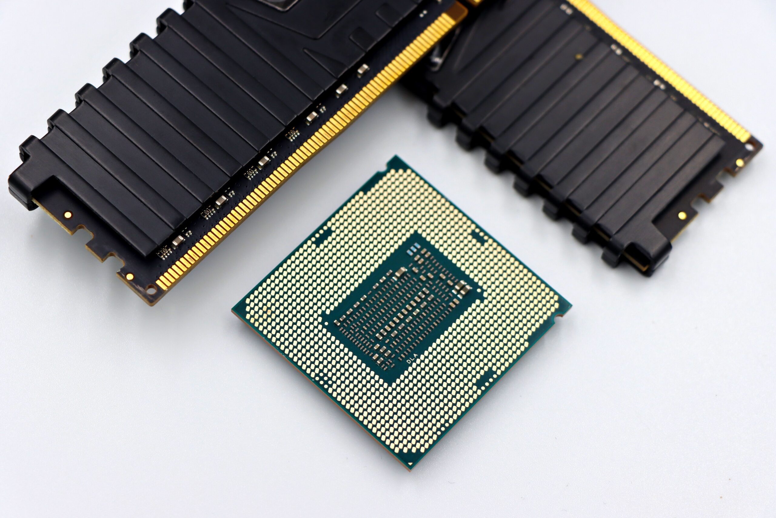
Every action on a computer—from rendering a video to calculating a spreadsheet—is orchestrated by a single, microscopic component: the Central Processing Unit (CPU). Often called the “brain” of the computer, the processor is a complex silicon engine that executes billions of instructions per second. Understanding how a processor works reveals the fundamental magic behind modern computing, from the simplest microcontroller to the most powerful server chip.
The Core Architecture: Transistors as Switches
At its most basic level, a processor is a dense collection of transistors. A transistor is a semiconductor device that acts as an electronic switch, either allowing current to flow (representing a binary 1) or blocking it (representing a binary 0). Modern CPUs contain billions of these switches, etched onto a silicon die using photolithography. The most advanced processors, like those built on a 3-nanometer process, pack over 20 billion transistors into an area smaller than a fingernail.
These transistors are not random; they are organized into logical structures called logic gates (AND, OR, NAND, NOR). Combinations of gates form more complex circuits, such as adders, multiplexers, and flip-flops, which store single bits of data. The entire computational ability of a processor emerges from the controlled toggling and connecting of these circuits.
The Fetch-Decode-Execute Cycle: The Heartbeat of Computation
The processor operates on a relentless, rhythmic cycle known as the Fetch-Decode-Execute cycle. This cycle is driven by an internal clock, which generates a steady electrical pulse. The clock speed, measured in gigahertz (GHz), dictates how many cycles occur per second. A 4.0 GHz processor performs roughly 4 billion cycles every second, though modern processors can often execute multiple instructions per cycle.
1. Fetch: The Control Unit (CU) sends a memory address to the system’s Random Access Memory (RAM) via the memory bus. The address corresponds to the location of the next instruction in the program. The RAM responds by sending the instruction data back to the processor, where it is stored temporarily in the Instruction Register.
2. Decode: The instruction, which is a binary sequence, is too cryptic for the processor to execute directly. The Decode Unit interprets this binary code. It determines what operation needs to be performed (e.g., “ADD,” “SUBTRACT,” or “LOAD”), which registers (the CPU’s ultra-fast internal memory) hold the data, and where the result should go. Complex instructions may be broken down into multiple simpler micro-operations at this stage.
3. Execute: The decoded instruction is now sent to the appropriate functional unit. This is the Arithmetic Logic Unit (ALU) for mathematical calculations (addition, subtraction, bitwise AND/OR) or the Floating-Point Unit (FPU) for decimal-number operations. The ALU uses circuits like the full adder to perform addition on binary numbers in nanoseconds. For a “LOAD” instruction, the result is simply a value moved from RAM into a register. The result is then written back to a register or sent to RAM for storage.
Registers: The CPU’s Scratchpad
Registers are the fastest memory in the computer hierarchy, built directly into the processor core. They are typically 64-bit wide in modern desktops (meaning they hold 8 bytes of data). Common registers include:
- Program Counter (PC): Holds the memory address of the next instruction to fetch. After a fetch, the PC automatically increments.
- Instruction Register (IR): Holds the currently fetched instruction.
- Accumulator (ACC): Stores intermediate arithmetic and logic results.
- General-Purpose Registers (GPRs): Used for temporary data storage by the programmer or compiler.
Because registers are physically close to the execution units, accessing them takes one or two clock cycles, while accessing main RAM can take 100 or more cycles. This speed disparity is why modern processors rely heavily on registers and caches.
Caches: Bridging the Speed Gap
RAM is far slower than a processor’s clock speed. To avoid wasting cycles waiting for data, CPUs integrate multiple levels of cache memory (L1, L2, L3). This cache is a small, high-speed SRAM (Static RAM) located on the silicon die.
- L1 Cache: The smallest and fastest (typically 32KB per core). It is split into separate caches for instructions (L1i) and data (L1d).
- L2 Cache: Slightly larger and slower (256KB to 1MB per core).
- L3 Cache: Shared across all cores, larger (8MB to 32MB) and slowest among caches, but still significantly faster than RAM.
The processor uses a prefetcher to predict which data will be needed next and loads it from RAM into these caches ahead of time. If data is found in the L1 cache (a “cache hit”), the processor avoids a slow trip to RAM. If it is not found (a “miss”), it checks L2, then L3, and finally fetches from RAM. Modern CPUs achieve hit rates above 90% in L1 for well-optimized code.
Pipelining: Overlapping Work for Speed
Fetching, decoding, and executing a single instruction one at a time is inefficient. Pipelining allows the processor to work on multiple instructions simultaneously, much like an assembly line. A classic 5-stage pipeline might have:
- IF: Fetch instruction 1.
- ID: Decode instruction 1 while fetching instruction 2.
- EX: Execute instruction 1 while decoding instruction 2 and fetching instruction 3.
- MEM: Access memory for instruction 1 while executing instruction 2.
- WB: Write back result for instruction 1.
Theoretically, a 5-stage pipeline can complete one instruction per clock cycle. Real-world pipelines on CPUs like Intel’s Core architecture have 14 to 20 stages, allowing extremely high clock speeds but introducing complexity, such as data hazards (when one instruction depends on the result of a previous one still in the pipeline) and control hazards (when a branch instruction changes the flow).
Superscalar and Out-of-Order Execution
Pipelining does not increase the work done per cycle. Superscalar architecture does. A superscalar processor has multiple execution units (e.g., two ALUs, one FPU, one load/store unit). The Instruction Decode stage can issue multiple independent instructions to these units in the same cycle.
Out-of-Order Execution (OoOE) takes this further. The processor reorders instructions to keep all execution units busy. For example, if Instruction A needs data from slow RAM, the processor skips it and executes Instructions B and C (which are independent) while waiting. The results are then temporarily stored, and the processor commits them to registers or memory in the original program order, ensuring correct behavior. This is managed by a complex structure called the Reorder Buffer (ROB).
Multi-Core and Simultaneous Multithreading
A single core can only do so much. Multi-core processors integrate two or more independent cores on a single die. Each core has its own L1 and L2 cache and control unit, allowing true parallel execution of programs. An 8-core CPU can handle eight different threads of execution simultaneously.
To squeeze more performance from each core, engineers use Simultaneous Multithreading (SMT) , called Hyper-Threading by Intel. SMT allows a single core to manage two or more threads. It uses duplicated sets of registers (architectural state) to trick the operating system into seeing one physical core as two logical cores. When one thread is stalled waiting for cache, the other thread can use the core’s execution units. SMT typically adds 20-30% performance in multi-threaded workloads.
Instruction Set Architecture (ISA): The Language
The processor understands a specific set of instructions, known as the Instruction Set Architecture. The two dominant ISAs are:
- x86/x86-64: Used by Intel and AMD for desktops and servers. It is a Complex Instruction Set Computer (CISC), meaning instructions can be variable-length and perform multiple operations in one command.
- ARM: Used by Apple, Qualcomm, and most smartphones. It is a Reduced Instruction Set Computer (RISC), with fixed-length instructions that are simpler and more power-efficient. Apple’s M-series chips use ARM architecture and have proven competitive with x86.
The microarchitecture (the physical layout of transistors, caches, and pipelines) is how a specific processor implements that ISA. For example, Intel’s Raptor Cove core and AMD’s Zen 4 core both execute x86 instructions, but their internal designs are completely different.
Thermal Design Power (TDP) and Heat Management
Executing billions of transistors switching at high frequencies generates immense heat. Heat is the enemy of performance; excessive temperatures cause electrons to leak, creating errors. The processor’s Thermal Design Power (TDP) , measured in watts, describes the maximum heat the cooling system must dissipate. Desktop CPUs range from 65W to 250W. Heat is managed via:
- Thermal Throttling: If the temperature sensor detects a peak, the processor reduces its clock speed and voltage to cool down.
- Dynamic Frequency Scaling (Turbo Boost): When the workload is light and thermal headroom exists, the processor automatically increases its clock speed above the base frequency for short bursts.
- Advanced Cooling: Heat sinks, heat pipes, vapor chambers, and liquid cooling systems physically conduct heat away from the die to fans.
The processor is not merely a “thing that computes.” It is a layered system of physics, logic, and predictive engineering—a self-regulating, adaptive engine that translates abstract human commands into precise electrical actions. Every click, every keystroke, every pixel rendered on a screen is the result of this silent, billion-cycle-per-second dance of electrons through silicon.